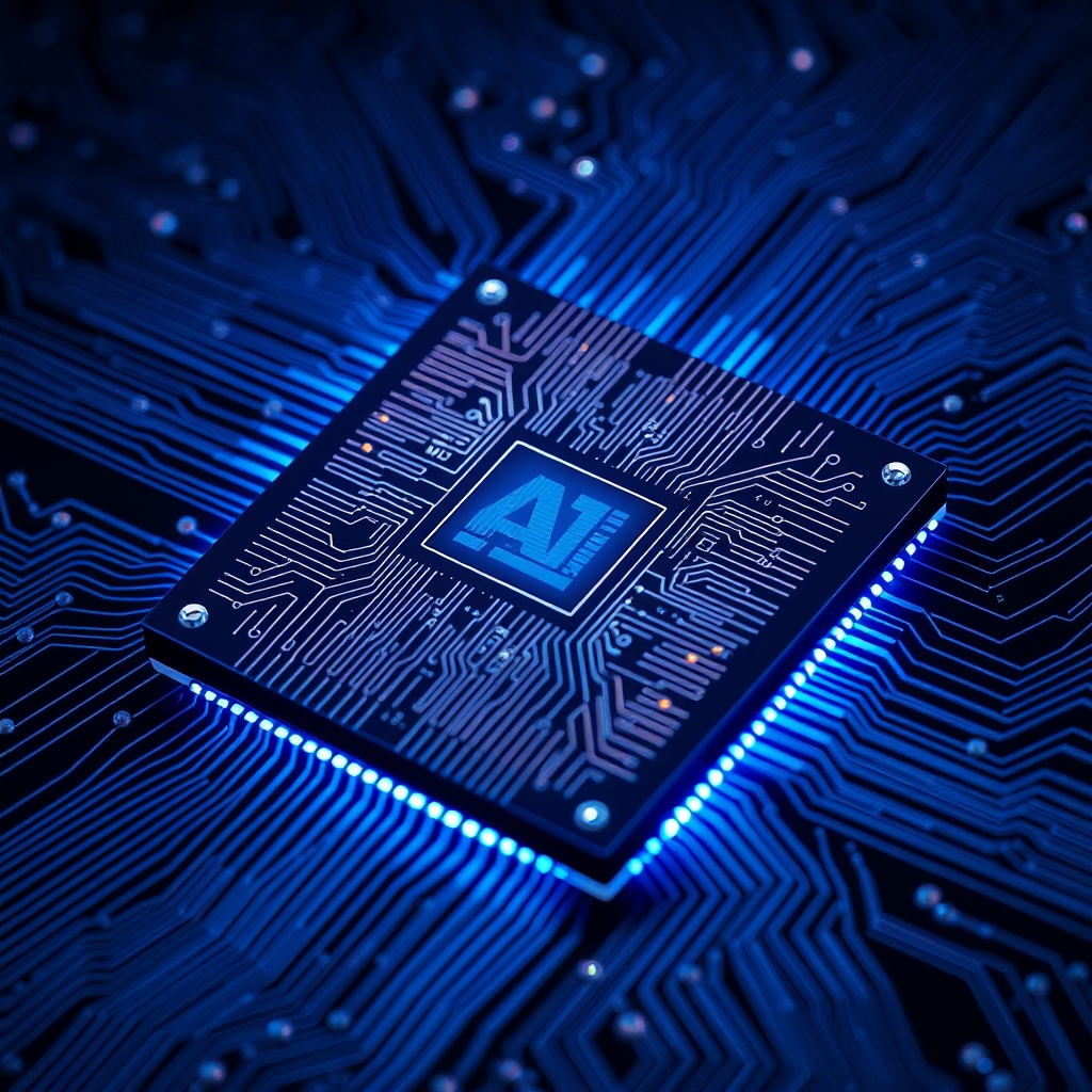
HBM's Evolution: Next-Gen Memory Redefining AI Computing
Recently, the semiconductor industry has faced diverse technological challenges alongside the rapid growth of artificial intelligence (AI). Among these, demand is increasing for integrating AI processors to maximize performance and efficiency—driving strong attention toward HBM (High Bandwidth Memory), a memory architecture that stands in a different league from conventional DRAM. Thanks to its ability to deliver both high-speed bandwidth and low power consumption, HBM plays a critical role in AI and GPU-based systems. Yet HBM is not merely an extension of memory capacity; it demands innovation at the architectural level. This article analyzes how HBM is evolving, and examines the technological challenges and opportunities it brings. Focusing particularly on advancements in next-generation HBM architectures and their impact on AI system design, the piece also offers a glimpse into the future of the semiconductor industry.
Technological Advancements in HBM: Higher Bandwidth and Integrated Performance
HBM (High-Bandwidth Memory) is a next-generation memory standard developed to surpass conventional GDDR memory. It leverages 3D packaging technology to vertically connect DRAM cells directly with the processor—unlike traditional planar interconnections. This vertical integration dramatically reduces data transmission distance between memory and processor, significantly boosting data transfer speeds. As a result, HBM has achieved bandwidths of approximately 35GB/s in the second generation and over 64GB/s in the third, far exceeding the first-generation benchmark of 20GB/s. This performance enables large-scale data processing essential for AI inference and training.
In particular, HBM3 and HBM3E—recently launched products—deliver more than three times the performance of their first-generation predecessors. Following HBM2E’s achievement of around 430GB/s, HBM3E now enables peak bandwidths exceeding 1.2TB/s. This technological leap has become a critical enabler for AI models to handle vastly larger parameter sets and process massive data streams in real time. However, as performance improves, so do challenges related to thermal management and packaging complexity.
Combining 3D NAND with HBM: A New Form of Memory Packaging
While 3D NAND and HBM were originally developed for different purposes, recent advancements have led to their convergence. 3D NAND was initially designed to increase storage capacity but is now being integrated with HBM in high-performance, large-scale AI systems to optimize memory hierarchy architecture—not merely increasing capacity but also enhancing access speed and bandwidth efficiency.
For example, HBM stores intermediate data requiring fast processing, while 3D NAND retains long-term machine learning model parameters. The resulting HBM + 3D NAND package has emerged as a core structural innovation that significantly boosts overall AI workflow efficiency. Particularly in systems designed for native AI processing, this integration offers dual advantages: minimizing data transmission paths and preserving programmability. As such, it has become a fundamental requirement in next-generation AI hardware design.
HBM’s Challenges: Manufacturing Complexity and Cost Pressures
Despite its exceptional performance, HBM manufacturing remains highly complex. The process demands precise 3D stacking at high temperatures and ultra-accurate interconnects linking the core to memory dies—challenges that lead to high production costs and low yield rates. Advanced variants like HBM3E require even greater precision, further impacting production scalability and delivery timelines. These issues pose significant burdens on mid-sized semiconductor companies.
Moreover, HBM’s high cost directly increases the total system expense of AI platforms. For instance, HBM2e used with NVIDIA’s A100 GPU costs more than three times as much as GDDR6, despite being relatively less expensive. This cost disparity creates substantial financial pressure for users building AI-specific servers or cloud infrastructure. Yet, the premium price reflects tangible gains in performance and energy efficiency—factors that can reduce long-term operational costs. Thus, HBM’s challenge extends beyond pricing: it now centers on achieving a sustainable balance between technological integration and cost efficiency.
The Next Generation of HBM: Becoming the Core Architecture of AI Systems
HBM has evolved beyond a mere memory technology to become a foundational computational architecture within AI systems. Thanks to large-capacity rank interfaces and high-speed interconnect designs, HBM nearly eliminates data transmission latency during AI model training and inference—making it a key solution for overcoming the performance limitations of traditional hardware.
Notably, direct package-on-package (PoP) integration between HBM and GPUs is poised to become the standard architecture for future AI systems. This design allows processors like CPUs or GPUs to access memory directly, maximizing data caching and parallel processing capabilities. Semiconductor companies are now heavily focused on such packaging techniques to achieve AI performance gains of over 200%.
Ultimately, HBM represents more than just memory expansion—it signifies a structural transformation in AI computing. It stands as one of the most critical milestones in the evolution of next-generation semiconductor industries.

Comments 0