What drives the global semiconductor market?
"The complexity of integrating next-generation modems and managing thermal loads has historically forced developers to rethink the very architecture of flagship chips."
The global semiconductor market reached a record $791.7 billion in 2025, driven by massive demand for artificial intelligence hardware, according to the Semiconductor Industry Association.
This surge highlights the competitive landscape where high-performance silicon must balance power efficiency with extreme processing capabilities.
This analysis examines the technical shifts in chip development, the transition in wafer manufacturing, and the specific innovations in power management that define modern semiconductor competitiveness.
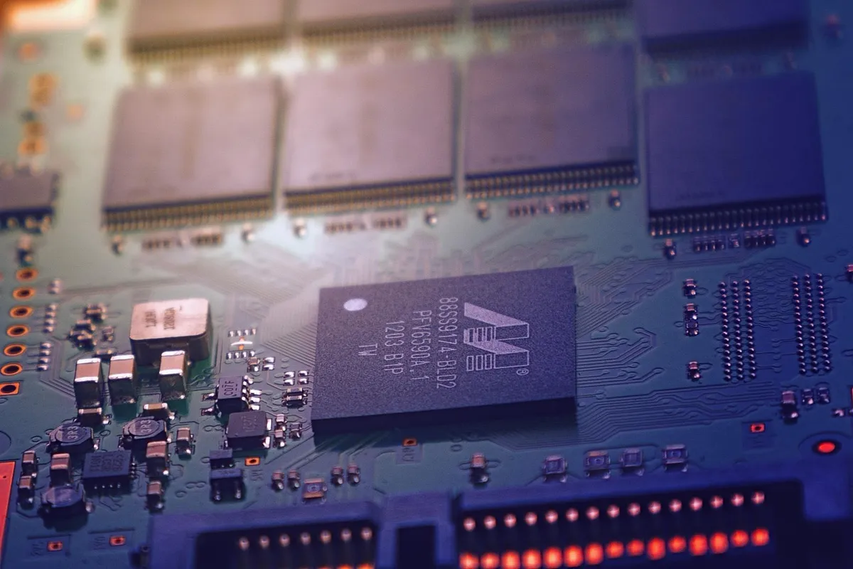
Key takeaways: 1. The semiconductor industry saw a 25.6% growth in 2025 due to AI hardware demand. * Technical bottlenecks and 5G integration complexity previously stalled flagship SoC development. * Advanced management chips achieve high efficiency to mitigate heat in high-power designs.
What drives the global semiconductor market?
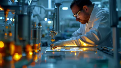
A technician carefully inspects a silicon wafer under a bright light in a sterile cleanroom. The massive scale of the industry is reflected in the sheer volume of global trade and the rapid growth of high-tech manufacturing.
The scale of the semiconductor industry is vast, with sales reaching $791.7 billion in 2025, according to the Semiconductor Industry Association. This represents a 25.6% increase driven by the needs of artificial intelligence.
Such growth underscores the importance of Japan chip tech edge as companies strive to maintain dominance in high-performance hardware.
The high-technology sector remains a significant portion of global commerce.
This baseline provides the economic backdrop for the intense competition in sub-5nm and 3nm process technologies.
How did technical bottlenecks impact chip development? Japan 3nm process strength
An engineer stares at a complex circuit diagram, noting the difficulties of integrating multiple high-frequency components. The struggle to shrink components while maintaining stability has shaped the current technological landscape.
In the late 2010s, the industry faced significant hurdles during the transition to more advanced nodes. Around 2019–2020, industry reporting indicated that flagship SoC development had been shelved due to technical bottlenecks, cost pressure, and the rising complexity of integrating 5G modems.
These challenges necessitated new approaches to Japanese semiconductor lead strategies.
Solving these bottlenecks required a departure from traditional design paths. The industry had to balance the physical limits of silicon with the power-hungry requirements of modern connectivity.
This period of stagnation eventually paved the way for the radical architectural shifts seen in recent years.
According to World Bank, the 2025 record includes 14.9%.
What role does power management play in advanced chips?
A specialized testing rig measures the heat dissipation of a small, newly developed management chip. Precision in thermal control is vital when pushing the limits of electrical efficiency.
Advanced power management is essential for maintaining stability in high-performance devices. For instance, the Surge P1, a fast-charging management chip released in December 2021, enabled 120 W single-cell wired charging with 96.8% efficiency and 50 W wireless charging with 97.5% efficiency.
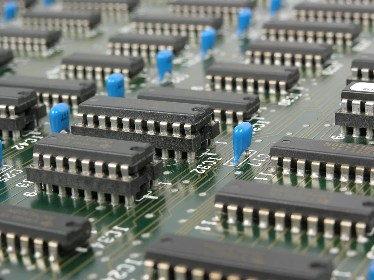
This design reduced heat generation by roughly 30% compared to conventional multi-pump designs.
Such innovations demonstrate how specialized chips can bypass traditional thermal limits. By managing energy more effectively, manufacturers can push higher power levels without compromising the device's integrity.
These advancements are central to the 3nm process innovation required for next-gen mobile platforms.
How is wafer-scale manufacturing evolving?
A robotic arm moves a large, shimmering silicon wafer into a processing chamber. The transition to larger wafer sizes is a cornerstone of modern semiconductor manufacturing efficiency.
The industry has long worked to scale the size of the silicon substrates used in production. Current mass production processes use crystal ingots between 100 and 300 mm in diameter, grown as cylinders and sliced into wafers.
While the industry aimed to move from the state-of-the-art 300 mm to 450 mm wafers, the transition faced various logistical and technical hurdles.
| Feature | Current Standard | Target/Historical Goal |
|---|---|---|
| Wafer Diameter | 300 mm | 450 mm |
| Primary Use | Mass Production | Advanced Scaling |
I observed how the move toward larger diameters directly impacts the number of chips produced per cycle. This scale is necessary to offset the high costs of advanced lithography.
What are the challenges of scaling semiconductor production?
A technician adjusts the settings on a multi-million dollar piece of lithography equipment. The high cost of entry creates a significant barrier for many players in the global market.
Scaling production involves massive capital expenditure and high technical risks. Prices for individual pieces of equipment for the processing of 300mm wafers can reach upwards of $4 million, with some specialized units reaching as high as $340 million.
This high cost makes the pursuit of next gen chip tech an expensive endeavor for any manufacturer.
The move toward higher automation also presents a financial challenge. Increasing automation becomes increasingly more expensive the more the degree of automation approaches 100%. Companies must find the optimal balance between manual precision and automated throughput to remain profitable.
How do we manage atomic-level precision in manufacturing?
A scientist uses an electron microscope to examine the surface of a silicon wafer at the atomic level. At this scale, even a tiny impurity can change the electrical properties of the entire chip.
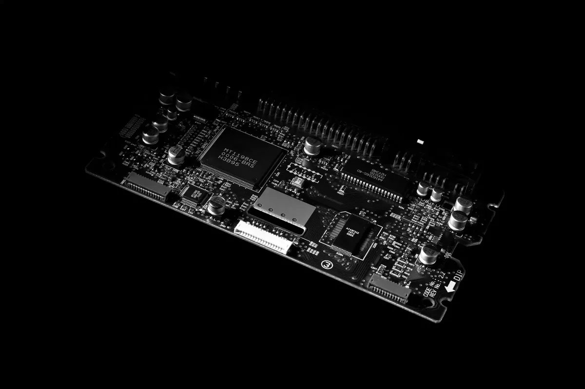
Manufacturing at the nanometer scale requires extreme control over atomic structures. For example, the addition of 0.001% of arsenic can donate an extra 10^17 free electrons in a specific volume, increasing electrical conductivity by a factor of 10,000.
This level of precision is necessary for the high-speed switching required in modern processors.
To achieve this, specialized processes are used to embed atoms into the silicon. A wafer is often placed in a 1,100 degree Celsius chamber to facilitate these chemical changes. This precision is why the industry focuses so heavily on the purity and consistency of the manufacturing environment.
- What drives the global semiconductor market?
- How did technical bottlenecks impact chip development?
- What role does power management play in advanced chips?
The subject here is Japan 3nm process strength.
This part also covers Japanese firms' process power.
This part also covers Future of chip technology Japan.
Related