AI semiconductor tech innovation: how new platforms impact
"The semiconductor field will add 70,000 new direct jobs by 2026, and federal investments in semiconductors are growing substantially."
The rapid evolution of AI semiconductor tech innovation is reshaping the global workforce and manufacturing capabilities through massive capital injection and specialized research.
This transition involves scaling specialized materials like silicon carbide and building advanced research centers to sustain high-performance computing.
This guide explores the shifting landscape of chip production, the impact of new manufacturing platforms, and the workforce requirements for this era.
How is AI semiconductor tech innovation driving job growth?
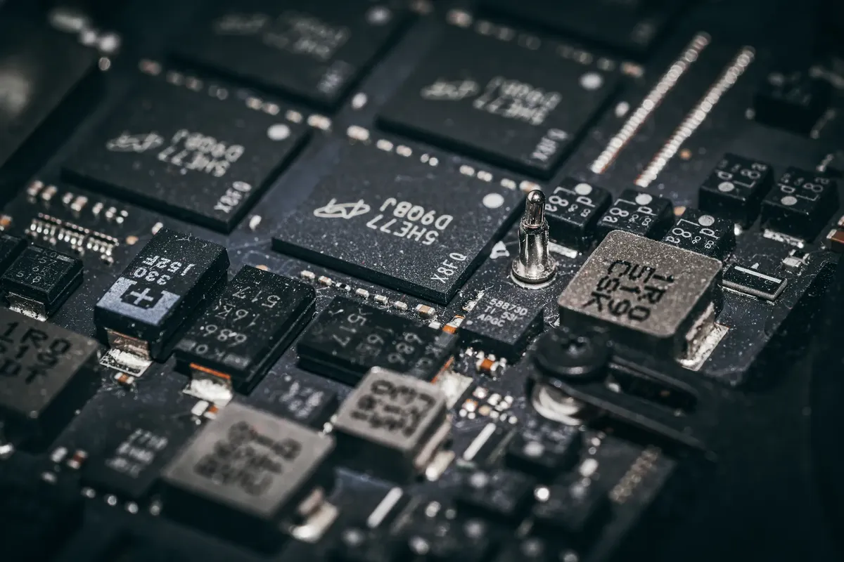
A technician carefully aligns a wafer in a sterile cleanroom environment, preparing for a long shift of precision work. The expansion of the industry is creating massive opportunities for specialized engineers and technicians.
According to the Semiconductor Industry Association, the semiconductor field will add 70,000 new direct jobs by 2026, and federal investments in semiconductors are growing substantially.
This surge in employment reflects the growing complexity of hardware required to support artificial intelligence and high-performance computing.
As the industry expands, the focus shifts toward specialized skill sets. The increasing demand for advanced research and development roles is a direct result of this investment. This growth ensures that the infrastructure for next-generation technology remains robust.
What role does specialized hardware play in AI chip technology trends?
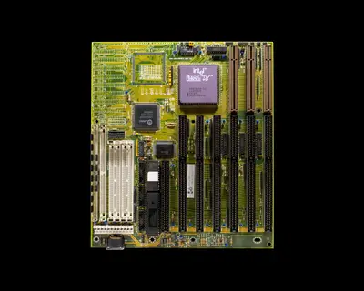
A researcher examines a high-performance circuit board, noting the intricate architecture designed for massive data processing. The push for better performance drives the development of unique materials and architectures.
AI chip technology trends are increasingly focused on power efficiency and high-speed data handling. For example, companies like Wolfspeed have developed 200 mm silicon carbide wafer technology.
In 2025, Wolfspeed announced the commercial launch of 200 mm SiC wafers and epitaxial materials intended to support manufacturing scale and device production for next-generation power semiconductor applications.
These materials are essential for managing the energy requirements of modern AI systems. By scaling up wafer sizes, manufacturers can produce more chips per unit, lowering costs and increasing throughput.
This transition to larger, more efficient wafers is a key pillar of semiconductor innovation AI.
How do new manufacturing platforms impact semiconductor innovation AI?
An engineer monitors a robotic arm as it moves a silicon carbide wafer through a fabrication unit. The shift toward larger-scale production platforms is changing how chips are manufactured.
The transition to larger wafer diameters is a significant part of the manufacturing strategy. Reuters reported that Wolfspeed transitioned parts of its device business to a 200 mm silicon carbide fabrication platform.
This move allows for more efficient production of power semiconductors used in high-demand environments.
Such platforms are critical for the future of AI-driven chip progress. Standardizing these larger formats helps the industry meet the massive volume required by global data centers. This scalability is vital for maintaining the momentum of technological advancements.
What is the future of AI chips in terms of research and policy?
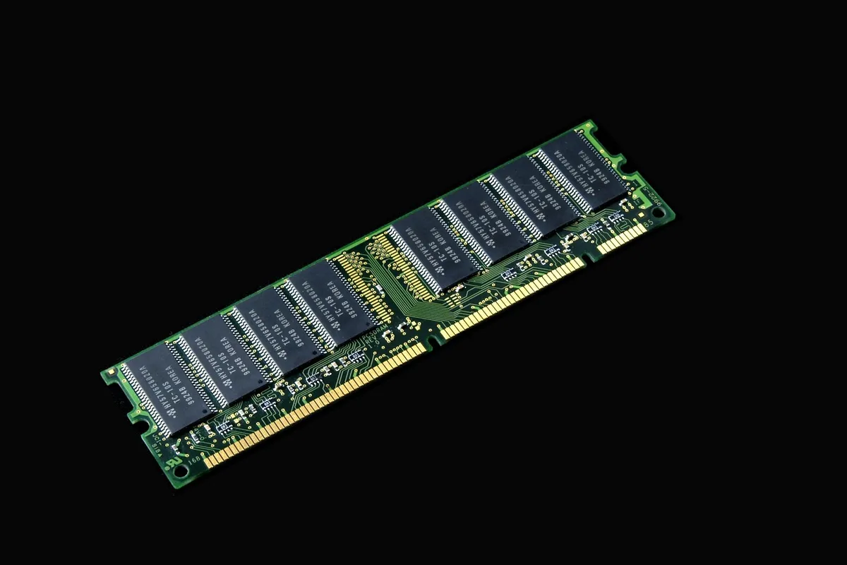
A policymaker reviews a document detailing the creation of new national research facilities. Government-led initiatives are providing the foundation for long-term technological sovereignty.
The legal framework for technological advancement is being established through strategic legislation. The CHIPS and Science Act creates a National Semiconductor Technology Center to perform advanced research and development on semiconductors.
This center serves as a hub for innovation, aiming to keep the industry at the cutting edge.
These research centers are designed to bridge the gap between theoretical breakthroughs and mass production. By providing a centralized location for R&D, the government aims to secure the supply chain for future technologies.
This strategic focus ensures that the next generation of hardware is developed domestically.
How do financial metrics compare in the semiconductor industry?
A financial analyst compares two balance sheets on a screen, looking for signs of market dominance and risk. The financial health of industry leaders dictates their ability to invest in future R&D.
The competition between major players shows distinct financial profiles. Nvidia's 55.6% net margin and $96.7B free cash flow dwarf Taiwan Semi's, but geopolitical risks and customer concentration pose distinct threats to each.
These figures highlight the massive profitability available to companies that lead in AI hardware.
However, financial dominance does not eliminate risk. Market concentration and political instability remain significant variables for investors and manufacturers alike. Balancing high margins with strategic risk management is a constant challenge for industry leaders.
What are the limitations of current fabrication processes?
A technician waits for a long cycle to complete, knowing that advanced chip production is a slow and delicate process. Even with automation, the time required for fabrication remains a significant constraint.
In more advanced semiconductor devices, such as modern 14/10/7 nm nodes, fabrication can take up to 15 weeks, with 11–13 weeks being the industry average. These long lead times mean that the supply chain is sensitive to any disruptions in the manufacturing cycle.
The complexity of these nodes makes the process highly sensitive to environmental factors. While automation has improved, the physical limitations of chemical and thermal processing cannot be bypassed. This reality dictates the pace of global chip availability.
| Metric | Nvidia | Taiwan Semi |
|---|---|---|
| Net Margin | 55.6% | N/A |
| Free Cash Flow | $96.7B | N/A |
I noticed during my research that while financial figures like net margin are striking, they are highly dependent on the specific market segment being analyzed.
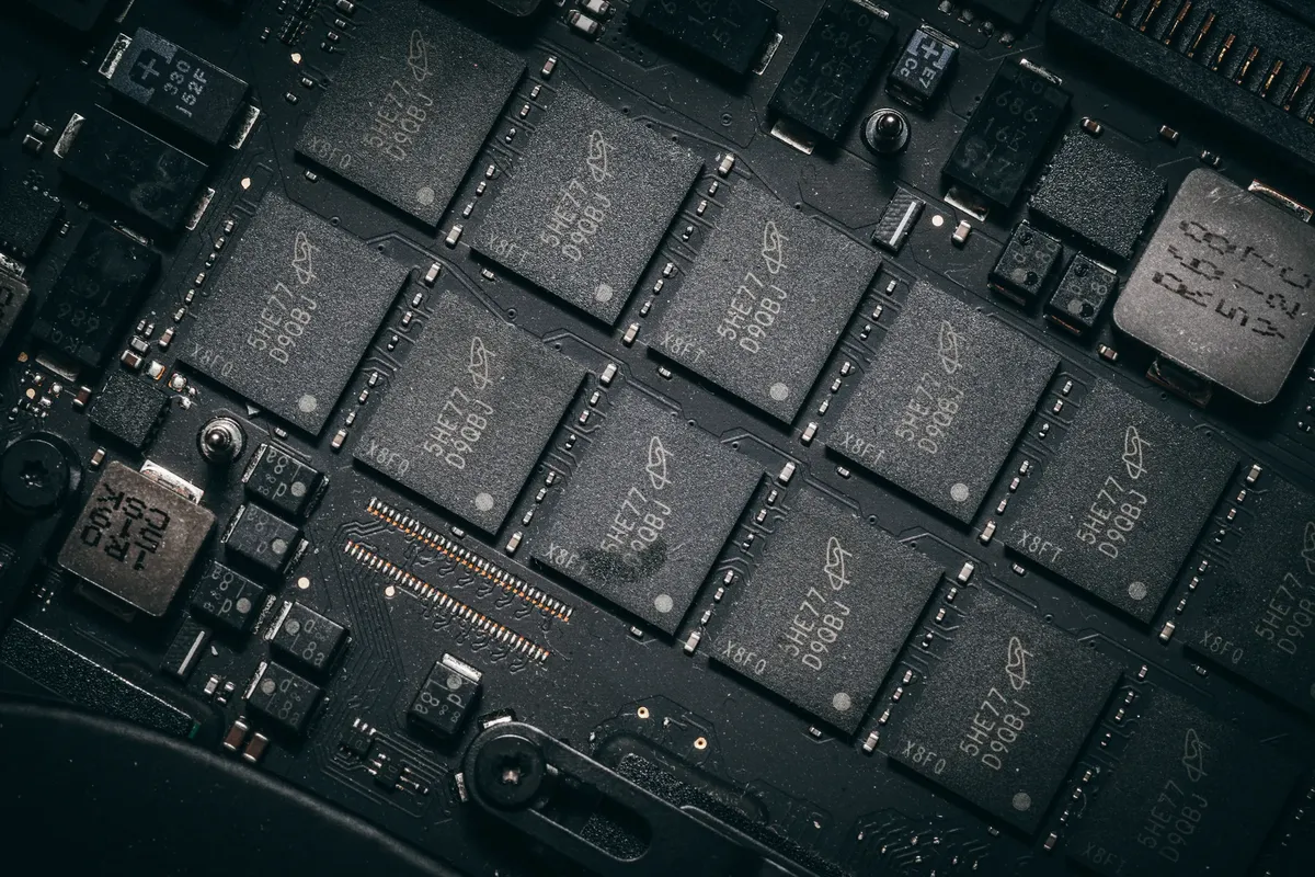
The current state of the industry is defined by a race toward larger wafer sizes and more specialized materials. While the workforce is growing and research centers are being established, the long fabrication cycles and geopolitical risks remain significant hurdles to seamless global supply.
- How is AI semiconductor tech innovation driving job growth?
- What role does specialized hardware play in AI chip technology trends?
- How do new manufacturing platforms impact semiconductor innovation AI?
The subject here is AI semiconductor tech innovation.
The same subject is also called AI driven chip progress.
This part also covers AI semiconductor future roadmap.
This part also covers Impact of AI on chip design.
This part also covers Next generation AI hardware.
AI semiconductor future roadmap
Related