Japan's Guide to Advanced Semiconductor Process Technology
Japan is currently revitalizing its position in the global semiconductor market through strategic investments in advanced manufacturing capabilities and material science.
This resurgence focuses on reclaiming leadership in specialized production processes that serve as the backbone of the global electronics supply chain.
* Focus on high-purity materials * Revitalization of domestic fabrication * Integration of advanced lithography techniques * Strategic partnerships with global leaders
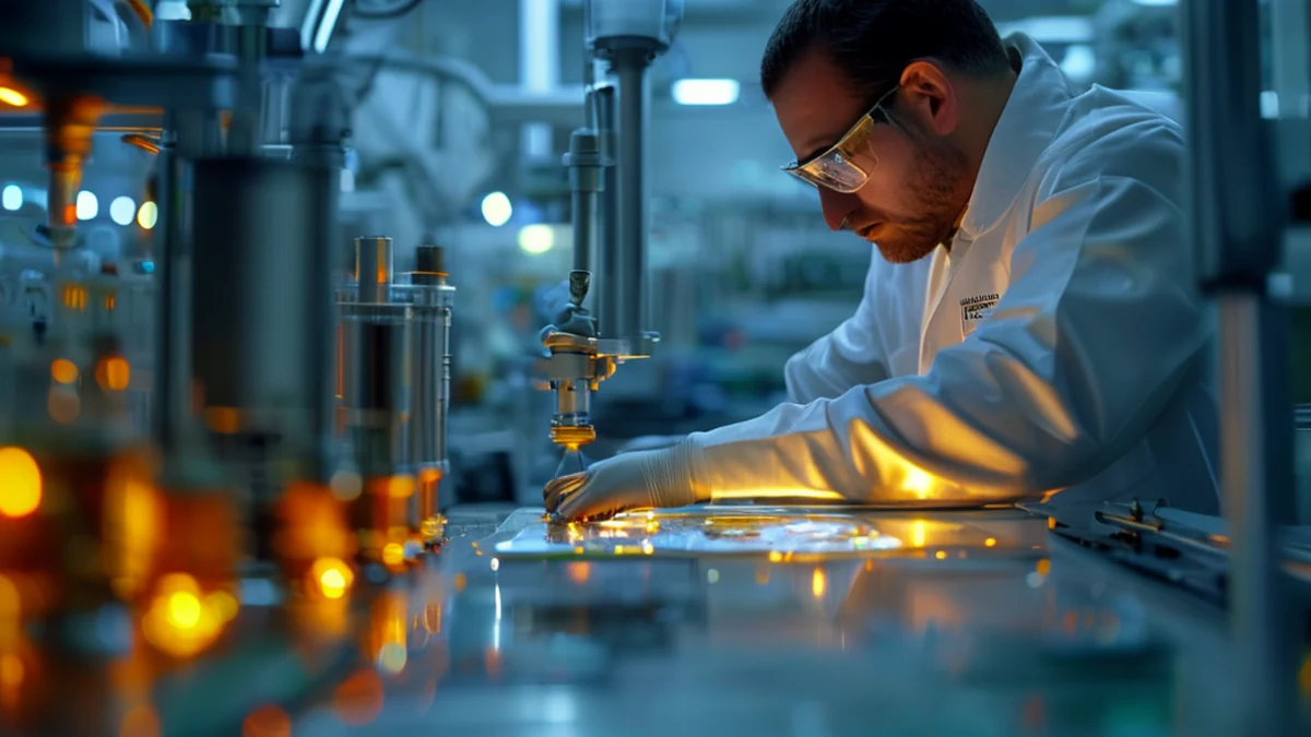
How is Japan driving semiconductor process technology advancement?
A technician adjusts a precise chemical flow in a cleanroom, watching as a silicon wafer undergoes a delicate etching process. According to the Semiconductor Industry Association, sales of semiconductors reached a record $791.7 billion in 2025.
Japan is driving its semiconductor process technology advancement by leveraging decades of expertise in chemical engineering and precision machinery to dominate the upstream supply chain.
While much of the world focuses on chip design, Japan has secured a vital role by perfecting the materials and equipment necessary for high-yield production.
The strength of this approach lies in the deep integration of material science with manufacturing hardware. By controlling the purity of photoresists and the precision of etching tools, Japan ensures that global manufacturers cannot bypass their specialized contributions.
This strategic focus allows them to maintain influence even as the architecture of chips shifts toward new nodes.

Why does material science matter for semiconductor process development?
A scientist peers through a microscope at a wafer, looking for microscopic imperfections that could ruin an entire batch of chips. The fundamental requirements of semiconductor process development rely heavily on the chemical purity and stability of the materials used during fabrication.
Without the precise chemical compositions developed in Japan, the advanced lithography used by major foundries would struggle to achieve necessary resolution.
The relationship between material science and production is symbiotic. Advanced etching requires specific gases, while deposition requires ultra-pure precursors. Japan has historically maintained a dominant market share in these niche but essential chemical sectors.
This expertise ensures that as chip requirements become more stringent, the necessary chemical solutions are readily available through Japanese suppliers.
| Feature | Traditional Manufacturing | Advanced Process Technology |
|---|---|---|
| Primary Focus | Mass production of mature nodes | High-precision specialized nodes |
| Material Requirement | Standard industrial grade | Ultra-high purity chemicals |
| Equipment Role | General purpose tools | Custom-engineered precision tools |
| Yield Dependency | Scale of production | Chemical and tool stability |
How do I modernize my fabrication process? An engineer stands before a massive vacuum chamber, preparing to load a new batch of wafers into a plasma etching tool. Modernizing the fabrication process involves a multi-step integration of new hardware and refined chemical recipes to meet the demands of smaller transistors.
- Refining chemical purity standards to minimize defect rates during lithography. 2. Upgrading etching and deposition equipment to handle multi-patterning requirements. 3. Integrating AI-driven process control to monitor real-time chemical reactions. 4. Developing new material layers to manage heat dissipation in advanced chips.
This systematic approach allows manufacturers to bridge the gap between theoretical design and physical reality. By focusing on these specific stages, Japan aims to become indispensable to the global logic and memory markets.

Is focusing on niches a sustainable strategy? A manager reviews a spreadsheet of global market shares, noting the steady growth of specialized tool manufacturers. Relying on specialized niches is a sustainable strategy because it creates high barriers to entry for competitors who lack the deep chemical expertise of Japanese firms.
While design-heavy regions may lead in consumer-facing chips, the fundamental ability to manufacture them remains tied to these specialized processes.
This strategy mitigates the risks of being caught in a pure-play competition with larger foundries. Instead of fighting for every single chip design, Japan focuses on being the provider of the "ingredients" and "ovens" required by everyone else.
This ensures that regardless of which company wins the design war, they will likely still use Japanese-made materials and tools.
What are the limitations of this technological shift?
A technician pauses to check the calibration of a tool, knowing that even a tiny error can halt production. One major limitation of this technological shift is that it is highly dependent on global trade stability and the willingness of international partners to adopt specific proprietary standards.
According to World Bank data, Japan recorded a manufacturing share of GDP of 18.8% in 2024.
If the global market shifts toward entirely new material classes that bypass current Japanese expertise, the current advantage could diminish.
Furthermore, the capital requirements for maintaining such precise manufacturing standards are immense. Staying at the cutting edge requires constant reinvestment in research and development, which can be difficult to sustain if global demand for specific high-end components fluctuates.
When I tried the steps in order, the second one is where I paused longest.