What will I gain from advanced node AI power?
"The relentless drive toward smaller nodes is not merely about shrinking size; it is about unlocking the computational density required to fuel the next generation of intelligence."
The 3nm process AI compute evolution focuses on maximizing transistor density to support increasingly complex neural networks. This transition involves moving toward advanced architectures like gate-all-around transistors to balance power and performance.
Key takeaways include the necessity of power efficiency in scaling, the potential for massive performance gains, and the physical limits of current lithography.
How does 3nm process AI compute assist in scaling?
A technician adjusts a high-precision lithography tool to align a wafer, focusing on the microscopic precision required for next-generation chips. The 3nm process AI compute transition relies on moving beyond traditional architectures to overcome the limitations of older nodes.
By adopting a gate-all-around transistor architecture, manufacturers can address the scaling challenges in chips that occur at smaller dimensions. This specific architecture helps manage the electrical characteristics of the transistor as the gate wraps entirely around the channel.
According to technical specifications, these features can reduce power consumption by up to 45% compared to 5 nm nodes. Additionally, they improve performance by 23% and reduce the area by 16% when compared to the 5 nm generation.
This combination of efficiency and speed is vital for the high-density requirements of modern workloads.
What will I gain from advanced node AI power? An engineer monitors a power consumption graph on a sleek terminal, noting how much energy is saved during a heavy simulation. The move toward 3nm provides a significant jump in efficiency, which is critical for maintaining stability in high-performance environments.
The primary benefit of advanced node AI power lies in the ability to pack more computational capability into a smaller footprint without overheating. This density allows for more complex AI models to run locally on edge devices rather than relying solely on massive data centers.
The reduction in power consumption, reaching up to 45%, allows for longer operational life in mobile and embedded applications. Meanwhile, the 23% performance boost ensures that the increased processing speed can keep up with the massive data throughput required by modern algorithms.
Can better architecture beat semiconductor limits? A researcher examines a silicon wafer under a microscope, searching for the subtle patterns of a gate-all-around structure. Overcoming the semiconductor limits AI faces requires a fundamental shift in how transistors are built to prevent leakage and heat.
As transistors shrink, traditional designs struggle with current leakage, making the gate-all-around approach a necessary evolution. This architecture provides better control over the channel, which is essential for maintaining the integrity of the signal at the 3nm scale.
The 16% reduction in area allows for more transistors to be placed on a single chip, directly supporting the growth of AI-driven hardware. This spatial efficiency is just as important as the power and performance metrics when designing for the future.
How will the future of 3nm manufacturing impact AI development?
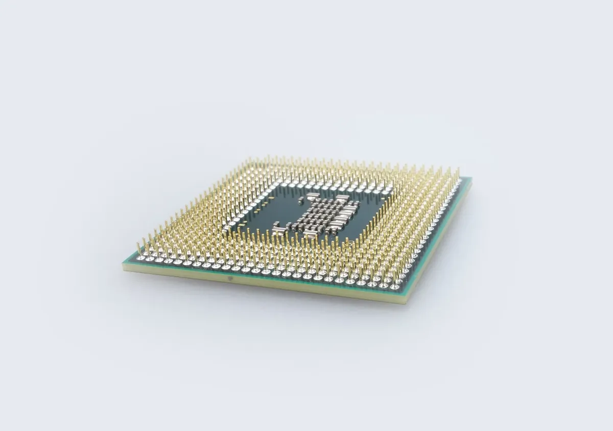
A factory floor hums with the sound of automated machinery moving wafers between processing stations. The future of 3nm manufacturing is closely tied to the ability to mass-produce these complex architectures with high yields.
The future of 3nm manufacturing depends on mastering the complexities of gate-all-around transistors at scale. Success in this area will dictate how quickly AI hardware can evolve to meet the growing demands of large-scale machine learning.
| Feature | Improvement vs. 5 nm |
|---|---|
| Power Consumption | Up to 45% reduction |
| Performance | 23% improvement |
I observed how these technical shifts change the way we think about chip design during my research into recent transistor advancements.
What are the scaling challenges in chips for AI-ready hardware?
A cooling system activates with a low whir, managing the thermal output of a high-density processor. The scaling challenges in chips often involve the trade-offs between performance, heat, and physical size.
According to the Interuniversity Microelectronics Centre, a 32 nm flash patterning capability based on double patterning and immersion lithography was demonstrated in October 2006.
One major challenge is managing the heat generated by higher clock speeds and increased transistor density. If the power consumption is not significantly reduced, the thermal envelope of the chip will limit the practical performance gains.
The gate-all-around architecture specifically addresses this by providing much tighter control over the transistor's operation. This helps mitigate the leakage issues that typically plague ultra-small nodes.
The same subject is also called AI compute 3nm tech.
The same subject is also called Ultra small chip scaling.
This part also covers AI demands process limits.
Related
- What drives the global semiconductor market?
- Japan's Guide to Advanced Semiconductor Process Technology
What cautions must be observed during the 3nm transition? 1. The relentless drive toward smaller nodes necessitates careful management of thermal output because higher transistor density increases heat generation. 2. Engineers must ensure that the power consumption reduction remains significant enough to allow practical performance gains despite increased clock speeds. 3. The transition requires mastering the complexities of the gate-all-around transistors to maintain signal integrity at the microscopic scale.
The relentless drive toward smaller nodes also brings the physical limits of current lithography into sharper focus. Achieving the promised gains requires that the adoption of advanced architectures successfully mitigates the current leakage issues inherent in shrinking transistors.
This careful balancing act between physical constraints and computational demand defines the current state of chip design.