What drives the need for advanced packaging technology?
"The future of computing lies in how we package the silicon that drives it."
The semiconductor industry is undergoing a massive shift toward advanced packaging to meet the demands of AI and high-performance computing. This transition involves complex manufacturing processes, significant capital investment, and a growing need for specialized engineering talent.
Key takeaways include the massive scale of recent industry investments, the importance of yield rates in advanced nodes, and the strategic shift toward domestic manufacturing and workforce development.
What drives the need for advanced packaging technology?
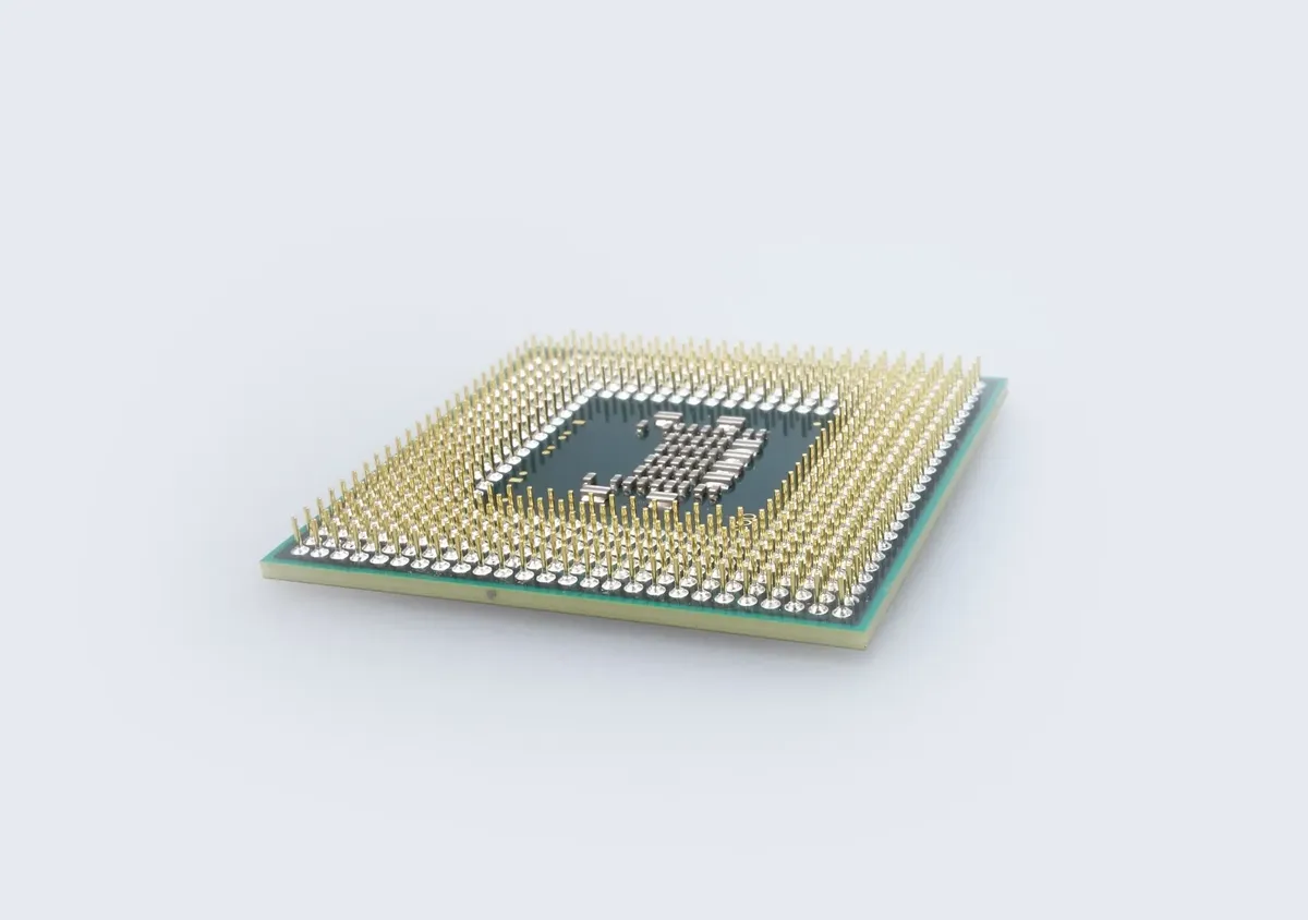
At midnight in the silent cleanroom, a technician's trembling hand guides the wafer as the hunger for performance drives the design.
A technician carefully aligns a wafer in a cleanroom, preparing for the delicate process of stacking dies.
This precision is essential as chips become larger and more complex, with some reaching potential sizes over 4,000 mm² when factoring in multiple compute dies and stacks of high-bandwidth memory.
The push for better performance is driving the industry toward more sophisticated assembly methods. Advanced packaging allows for higher density and better power efficiency, which are critical for AI-driven hardware.
As chip designs grow in size and complexity, the ability to integrate different components into a single package becomes a primary competitive advantage.
The industry is moving toward more integrated solutions to handle the massive data requirements of modern processors. This shift necessitates new tools and equipment capable of managing much larger silicon surfaces.
- Identify performance bottlenecks in traditional chip designs.
- Integrate heterogeneous components into a single package.
- Optimize thermal and electrical interconnects.
- In this sequence, the first step is the most critical.
How do manufacturing yields impact the success of new nodes?
An engineer monitors a digital readout, watching the percentage of functional chips produced from a single wafer. This metric is the lifeblood of semiconductor profitability and scaling.
Yield rates are a critical factor when transitioning to smaller, more advanced process nodes. For instance, reports indicate that while some manufacturers achieve near 90% yield on 3 nm production, others may face significantly lower results, such as roughly 50% yield during design-reuse.
These variations directly affect the cost and availability of high-end chips.
A low yield means that a significant portion of the chips on a wafer may not work as intended, sometimes falling as low as 30%. Maintaining high yields is essential for making advanced technology commercially viable.
How is the industry addressing labor and infrastructure needs?
A group of students in a high-tech lab works on specialized equipment, preparing for careers in the semiconductor sector. The classroom environment reflects the growing intersection of education and industrial necessity.
The massive scale of semiconductor projects requires a robust workforce and physical infrastructure. To support this, the CHIPS Act has led to more than 50 projects worth more than $200 billion, which are expected to create 44,000 jobs.
Such large-scale investments require a steady pipeline of trained engineers to maintain operations.

The talent gap is being addressed through both academic programs and strategic funding. For example, in May 2022, Purdue University launched the nation's first comprehensive semiconductor degrees program in anticipation of the CHIPS Act.
| Metric | Value |
|---|---|
| CHIPS Act Project Value | Over $200 billion |
| Projected Job Creation | 44,000 jobs |
I observed how these massive investment figures highlight the sheer scale of the global effort to secure chip supply chains.
What are the strategic investments in packaging equipment?
A specialist examines a new piece of lithography equipment, ensuring it meets the tight tolerances required for sub-2nm development. The equipment represents the cutting edge of manufacturing capability.
Companies are actively investing in the tools required for next-generation packaging to stay ahead of the curve. In early July, Applied announced a strategic stake in BE Semiconductor Industries (Besi), a Dutch advanced packaging equipment firm, acquiring approximately 9% of Besi’s shares.
This move highlights the importance of securing specialized equipment for advanced assembly.
These investments ensure that manufacturers have access to the most advanced technology for scaling. Such strategic moves are vital for maintaining a competitive edge in the global market.
How do different manufacturing nodes compare in performance?
A scientist compares two different silicon wafers, noting the subtle differences in density and power consumption. The comparison is a routine but vital part of the development cycle.
Newer nodes offer significant improvements over previous generations in terms of density and power. According to a paper Intel presented, the 18A node offers more than 30% logic density scaling and up to approximately 20% higher performance, or 36% power reduction, compared to the 2023 Intel 3 node.
These incremental gains are vital for the evolution of computing.
The trade-off between performance and power reduction is a central theme in node development. As nodes shrink, managing these variables becomes increasingly complex.
What are the limitations of current semiconductor scaling?
A researcher looks at a microscopic image of a wafer, identifying potential defects that could impact yield. The reality of manufacturing often clashes with the theoretical limits of physics.
Scaling technology faces significant challenges, particularly regarding yield and the physical limits of silicon. While advancements like the 18A node promise higher performance, the difficulty of achieving high yields at smaller nodes remains a constant hurdle.
These technical limitations can dictate the speed of industry-wide adoption.
A significant limitation is that manufacturers are typically secretive about their yields, making it difficult to verify the true success of a new process across the entire industry.

Wikipedia: CHIPS and Science Act Based on the retained excerpt mentioning National Science Foundation: $24 billion would go to a new 25 percent advanced semiconductor manufacturing tax credit to encourage firms to stay in the United States, and $200 million would go to the National Science Foundation to resolve short-term labor supply issues.
Wikipedia: CHIPS and Science Act Based on the retained excerpt mentioning Indiana and Purdue University: In July 2022, SkyWater announced plans to build an advanced $1.8 billion semiconductor manufacturing facility with the government of Indiana and Purdue University to pursue CHIPS funding.
Hanmi Semiconductor AI packaging success
The subject here is Hanmi Semiconductor AI packaging success.
The same subject is also called AI advanced packaging test.
The same subject is also called Next gen chip packaging.
Related