How are TSMC advanced AI nodes being deployed globally?
"The future of silicon is not just about smaller transistors, but about the massive scale of global manufacturing capability."
TSMC is expanding its technological footprint to meet the rising demands of the AI era through massive capacity and advanced process nodes. This transition involves moving from legacy nodes to cutting-edge 3nm technology while scaling global manufacturing facilities.
Key takeaways include the company's dominant market share, its massive global wafer capacity, and significant infrastructure investments in new regions like Arizona.
How does TSMC maintain a lead in the semiconductor foundry market?

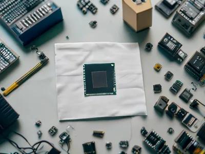
A technician carefully inspects a silicon wafer under a high-powered microscope in a sterile cleanroom. The company holds a commanding majority in the semiconductor foundry market, accounting for approximately 70% of the global market share.
This dominance allows the firm to set the pace for the entire industry.
This high market share provides the necessary capital to reinvest in next-generation technologies.
Such stability is reflected in the company's historical performance, where since 1994, TSMC has had a compound annual growth rate (CAGR) of 17.4 percent in revenue and a CAGR of 16.1 percent in earnings. These figures represent the strength of its foundry business.
The scale of operations is vast, involving highly specialized equipment and massive cleanrooms. The company's footprint is essential to the global economy, as TSMC constitutes about 30 percent of the Taiwan Stock Exchange's main index.
This level of integration ensures that its technological shifts impact the global market immediately.
- Continuous reinvestment in R&D to refine lithography processes.
- Scaling production capacity to meet global demand.
- Maintaining a diverse ecosystem of design partners.
What is the current scale of TSMC AI chip tech 2026?
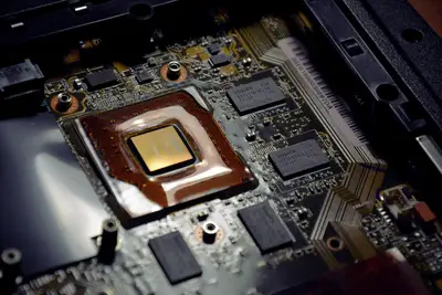
An engineer monitors a fleet of automated machines processing thousands of wafers simultaneously. As of 2020, TSMC has a global capacity of about thirteen million 300 mm-equivalent wafers per year. This capacity is vital for meeting the surge in demand for specialized processors.
The production range is diverse, covering a wide spectrum of needs. The company produces chips for customers with process nodes from 2 microns to 3 nanometres. This range allows it to support everything from legacy industrial applications to the most advanced AI hardware.
Meeting the needs of the future requires significant logistical and technical preparation. In 2011, the company planned to increase research and development expenditures by almost 39 percent to NT$50 billion to fend off growing competition.
It also planned to expand capacity by 30 percent in 2011 to meet strong market demand.
In this sequence, the second step is the most extensive.
How are TSMC advanced AI nodes being deployed globally?
A shipping container is loaded with specialized equipment destined for a new manufacturing site in the United States.
To diversify its geographic presence, the US Commerce Department later agreed to provide $6.6 billion in direct funding and up to $5 billion in loans to TSMC for the purposes of creating semiconductor manufacturing facilities in Arizona under the CHIPS and Science Act.

Expanding these nodes requires a massive shift in supply chain management. This geographical expansion aims to mitigate risks associated with localized production. By building in Arizona, the company integrates its advanced nodes into a broader global supply chain.
The move is a strategic response to the shifting landscape of semiconductor manufacturing. While the company remains centered in its home region, these new facilities represent a significant step in globalizing its production.
This ensures that its 2026 chip manufacturing capabilities are not limited to a single location.
How does 2026 chip manufacturing relate to economic stability?
A stock trader watches the fluctuating numbers on a digital terminal in a busy financial district. The economic impact of the semiconductor industry is profound, as Taiwan's exports of integrated circuits amounted to $184 billion in 2022, nearly 25 percent of Taiwan's GDP.
This economic weight makes the company's success a matter of national interest. The stability of the semiconductor sector provides a foundation for broader economic health. As the industry moves toward more complex AI-specific chips, this relationship becomes even more critical.
The interplay between technology and finance is constant. Because the company is so central to its home economy, any shift in its technological roadmap has immediate financial implications. This makes the pursuit of TSMC next gen technology a high-stakes endeavor for investors and governments alike.
What are the requirements for TSMC next gen production?
A scientist adjusts the laser settings on an EUV lithography machine to ensure precision. Scaling to advanced nodes requires massive capital and specific technological breakthroughs. The company must balance the high cost of R&D with the necessity of staying ahead of competitors.
To manage these requirements, the company follows a structured approach to growth:
- Continuous reinvestment into research and development to maintain node leadership. 2. Strategic expansion of manufacturing facilities to meet global demand. 3. Diversification of production sites to secure the global supply chain.
A final check of the production output ensures that every wafer meets the rigorous standards required for high-performance computing. I observed how these steps are essential for maintaining the precision required at the 3nm level.
What are the limitations of current AI semiconductor reliability?
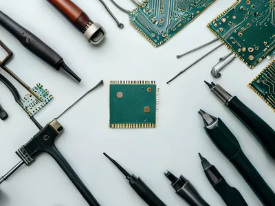
A quality control specialist examines a single chip for microscopic defects. While the company has achieved massive scale, it faces challenges related to the physical limits of silicon. Maintaining high yields at the 3nm level remains a complex engineering task.

The limitations of these processes are often tied to the extreme precision required at such small scales. For example, the complexity of EUV 3nm scaling presents significant manufacturing hurdles. These technical challenges represent the primary barrier to even more aggressive scaling.
The ability to maintain reliability while increasing density is the central challenge of the industry. As nodes shrink, the margin for error becomes nearly non-existent. This makes the management of global capacity and precision a constant struggle against the laws of physics.
The subject here is TSMC AI chip tech 2026.
The same subject is also called TSMC next gen AI.
This part also covers TSMC supply chain AI.
This part also covers Future of chip making.
Related