How does AI-driven demand shape the semiconductor market?
"The evolution of semiconductor assembly and testing is no longer just about hardware; it is about the structural integrity of the intelligence era."
The rise of AI-driven computing has forced a shift toward advanced packaging solutions to handle increased data speeds and power requirements. This transition requires specialized equipment and processes to integrate complex chip architectures into functional units.
This article explores the technological shifts in the semiconductor sector, the role of major industry players, and the market implications of advanced packaging.
How does AI-driven demand shape the semiconductor market?
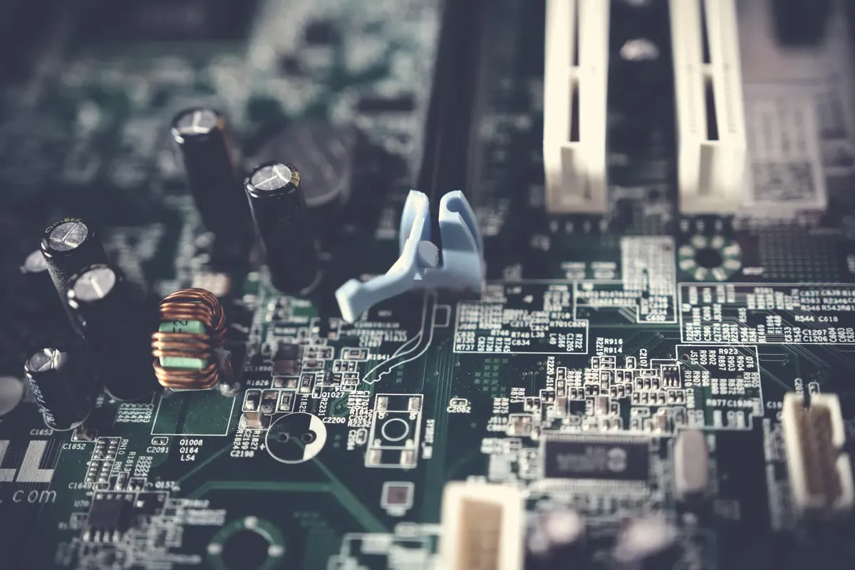
A technician adjusts a high-precision bonding machine in a sterile cleanroom, preparing for a delicate substrate placement. The demand for high-performance computing is driving a massive shift toward specialized manufacturing techniques.
According to the Singapore Economic Development Board, Singapore is set to increase investments to maintain its leadership in advanced manufacturing sectors like semiconductors.
As AI models grow in complexity, the physical limits of traditional chip designs necessitate advanced packaging solutions. These solutions allow for more efficient data transfer and power management between chiplets.
The industry is shifting from single-die designs to multi-die architectures that rely on sophisticated interconnect technologies.
This shift affects the entire supply chain, from equipment manufacturers to testing facilities. Companies must adapt to these new requirements to maintain a competitive edge in a rapidly changing landscape.
The global focus on semiconductor leadership is driving significant investment into these specialized manufacturing processes.
How will OSAT providers shape this tech shift? Korea US semiconductor AI packaging An engineer monitors a series of automated testing units that cycle through thousands of wafer samples per hour. Large-scale production facilities rely on specialized service providers to manage the complexity of modern chip assembly.
The Outsourced Semiconductor Assembly and Test (OSAT) sector is a critical component of the semiconductor ecosystem. These providers manage the intricate processes of packaging and testing that follow wafer fabrication.
As chip designs become more complex, the technical requirements for OSAT providers increase significantly.
This concentration of expertise allows major players to lead the way in developing new packaging standards.
Their ability to scale complex processes is essential for meeting the volume demands of the AI era.
How is advanced packaging technology evolving?
A researcher examines a microscopic cross-section of a multi-layered chip structure under a high-powered lens. The move toward three-dimensional stacking is changing how engineers approach chip design and thermal management.
Advanced packaging involves techniques like chiplet integration and through-silicon vias to create more compact and powerful devices. This approach allows different types of chips to be combined into a single package, optimizing performance for specific applications.
The goal is to overcome the limitations of traditional scaling by adding functionality through packaging.
The technical standards for these processes are often documented in specialized scientific literature.
For instance, IEEE Transactions on Advanced Packaging is a quarterly peer-reviewed scientific journal published by the IEEE Components, Packaging & Manufacturing Technology Society and the IEEE Photonics Society.
Such publications help define the rigorous standards required for next-generation electronic assembly.
Who stands to gain from assembly innovations? A logistics manager reviews a digital dashboard showing the global movement of electronic components across continents. The ripple effects of packaging innovation reach every corner of the global electronics industry.
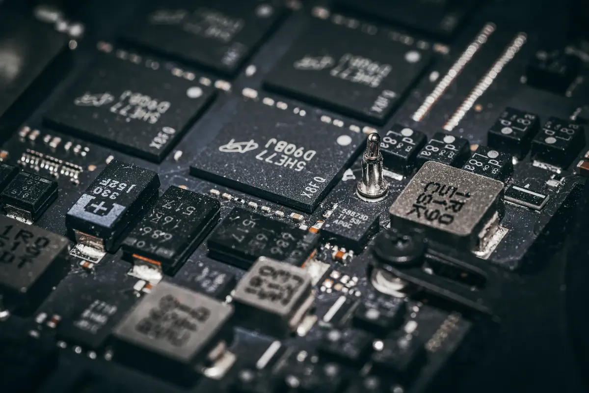
The benefits of these technological leaps extend to various sectors, including consumer electronics, automotive, and data centers. Improved packaging leads to more efficient, smaller, and more powerful devices for end-users.
Companies that master these techniques can offer superior performance in a crowded market.
| Feature | Traditional Packaging | Advanced Packaging |
|---|---|---|
| Architecture | Single-die focus | Multi-die / Chiplet integration |
| Complexity | Lower interconnect density | High-density 2.5D/3D stacking |
I observed how these different architectural approaches change the physical footprint of the final product during a recent industry comparison. The table above highlights the primary technical distinctions between the two methods.
What are the challenges of scaling these new processes?
A quality control specialist uses a specialized sensor to check for microscopic cracks in a newly assembled module. Scaling sophisticated packaging techniques from the lab to mass production presents significant engineering hurdles.
One major challenge is maintaining reliability across thousands of interconnected components within a single package. Thermal management becomes increasingly difficult as chips are stacked closer together.
Ensuring consistency in yield during high-volume manufacturing is also a constant struggle for producers.
A limitation of these advanced processes is that they require extremely high capital investment and specialized cleanroom environments to prevent contamination. This can create barriers to entry for smaller manufacturers.
- How does AI-driven demand shape the semiconductor market?
- How will OSAT providers shape this tech shift?
- How is advanced packaging technology evolving?
The subject here is Korea US semiconductor AI packaging.
The same subject is also called AI packaging tech advance.
The same subject is also called Semiconductor advanced packaging.
The same subject is also called Korea US chip innovation.
The same subject is also called Advanced electronic packaging.
This part also covers Impact of AI packaging on market.
This part also covers New semiconductor process breakthroughs.
This part also covers Future of advanced chip technology.
Impact of AI packaging on market
Related