ASML lithography monopoly: Why co-investment secured future
"The future of microchip manufacturing is shaped by the precision of light and the scale of industrial investment."
The global semiconductor landscape is defined by the specialized tools required to print microscopic circuits, a field where ASML lithography monopoly remains a central factor. This dominance is built on strategic co-investment from major chipmakers and high-level political goals in Europe.
This article explores the history of these investments, the technical drivers behind them, and the strategic commitments made to maintain global supply chains.
Key takeaways: * Early co-investment programs secured the technological future of lithography. * Strategic stakes from Intel, Samsung, and TSMC facilitated advanced wafer transitions. * European political goals aim to significantly increase regional semiconductor production.
How did early investments shape the ASML lithography monopoly?

A boardroom in 2012 saw the strategic movement of capital that would define the next decade of silicon. To ensure the long-term viability of advanced lithography, ASML launched a co-investment program in 2012.
Under this specific arrangement, 23 percent of the company was sold to its three largest customers: Intel, TSMC, and Samsung.
This move was designed to align the interests of the toolmaker with the world's leading chip manufacturers. By spreading ownership, the company secured the capital and the technical roadmaps necessary for future breakthroughs.
This period of restructuring laid the groundwork for the current state of the industry.
The co-investment was not merely about capital but about technical roadmaps. In July 2012, Intel purchased a 15 percent stake in ASML in exchange for $4.1 billion.
This specific investment was stated to accelerate Intel's transition from 300 mm to 450 mm wafers as well as support further development of EUV lithography.
Samsung and TSMC also bought stakes in the firm under this same co-investment program. These partnerships ensured that the most advanced lithography tools would be developed in tandem with the manufacturing needs of the industry's largest players.
This integrated approach helped solidify the semiconductor tool monopoly.
What drove the push for advanced lithography technology?
A technician in a cleanroom adjusts a lens, focusing on the precision required for next-generation wafers. The push for advanced lithography was driven by the need to scale transistor density and manage power consumption. The 2012 investment from Intel was a key catalyst in this technical race.
The $4.1 billion investment in July 2012 was intended to push the boundaries of wafer sizes and light-based etching. This move was stated to accelerate Intel's transition from 300 mm to 450 mm wafers as well as support further development of EUV lithography.

Such technical leaps are essential for maintaining the pace of Moore's Law.
The scale of these machines is massive, yet they operate on a microscopic level. While the industry moved toward smaller nodes, the physical requirements for lithography grew increasingly complex. The co-investment provided the financial stability to tackle these engineering hurdles.
The pursuit of higher precision often involves pivoting between different manufacturing standards. In November 2013, ASML paused development of 450 mm lithography equipment, citing uncertain timing of chipmaker demand.
This decision highlighted the delicate balance between long-term research and immediate market realities.
How does Europe plan to maintain EU semiconductor leadership?
A diplomat walks through a high-tech manufacturing hub in Europe, contemplating the future of regional autonomy. The European Union has long sought to bolster its position in the global supply chain. This ambition is reflected in recent political announcements regarding domestic production.
In July 2021, European Commissioner Thierry Breton, visited ASML and announced a goal of at least 20 percent of global production of semiconductors in Europe by 2030. This target is supported via a European Alliance on semiconductors.
The goal is to ensure that Europe remains a vital node in the global electronics ecosystem.
Strengthening the local ecosystem requires both technical talent and industrial infrastructure. The European Alliance on semiconductors aims to foster the necessary research and manufacturing capabilities.
This strategic focus is intended to protect the EU semiconductor leadership in an increasingly competitive global market.
The presence of industry leaders in Europe provides a foundation for these ambitious goals. While the global market is vast, the concentration of high-end lithography expertise in Europe is a significant strategic asset. This expertise is central to the continent's industrial identity.
What are the requirements for global market access?

A logistics manager inspects a shipment of precision components destined for a North American facility. To maintain a presence in the United States, companies must navigate complex regulatory and supply chain requirements. These commitments often involve localized research and sourcing.
To maintain its standing in the global market, ASML has had to align with specific regional interests.
Furthermore, in return for being permitted to join this consortium, ASML committed to the establishment of a US-based research center and to source 55 percent of components for all machines sold in the US from American suppliers.
These commitments ensure that the technology is not just developed in one region but is integrated into the supply chains of its primary markets. The requirement to source a majority of components from American suppliers is a specific condition of its market access.
This helps distribute the technological footprint.
The establishment of a US-based research center also ensures that technical innovation remains globally distributed. This allows for closer collaboration with American semiconductor firms. Such measures are vital for managing the geopolitical complexities of the semiconductor industry.
How do these factors contribute to the ASML technological advantage?
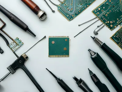
An engineer examines a complex circuit pattern, noting the precision achieved through advanced lithography. The combination of strategic investment, political support, and localized supply chains creates a unique position in the market.
This multi-faceted approach is what sustains long-term dominance.
The early co-investment program was a masterstroke in securing the future. By selling 23 percent of the company to Intel, TSMC, and Samsung in 2012, the firm ensured its customers were also its partners. This created a symbiotic relationship that is difficult for competitors to replicate.

The technical focus on EUV lithography was also a defining factor. The $4.1 billion investment in July 2012 was specifically aimed at supporting the development of EUV. This technology is a cornerstone of modern high-end chip manufacturing.
| Investment Type | Primary Objective |
|---|---|
| 2012 Co-investment | Secure customer alignment and technical roadmaps |
| Intel $4.1B Stake | Accelerate wafer transition and EUV development |
I observed how these early strategic decisions directly enabled the high-precision tools used in fabs today. The scale of the ASML technological advantage is built on these historical foundations.
Wikipedia: ASML (full) Based on the retained excerpt mentioning European Alliance: In July 2021, European Commissioner Thierry Breton, visited ASML and announced a goal of at least 20 percent of global production of semiconductors in Europe by 2030, and support via a European Alliance on semiconductors.
- How did early investments shape the ASML lithography monopoly?
- What drove the push for advanced lithography technology?
- How does Europe plan to maintain EU semiconductor leadership?
Related